Contents
- 🔍 Introduction to Wafer Preparation
- 💡 History of Wafer Preparation
- 📈 Evolution of Wafer Sizes
- 🔬 Wafer Cleaning and Etching
- 📊 Wafer Inspection and Metrology
- 🚀 Wafer Preparation for Advanced Nodes
- 🤝 Collaboration and Standardization
- 📊 Economic Impact of Wafer Preparation
- 🌎 Environmental Considerations
- 🔮 Future of Wafer Preparation
- 📝 Conclusion
- Frequently Asked Questions
- Related Topics
Overview
Wafer preparation is a critical step in the production of semiconductors, involving the growth, slicing, and polishing of silicon wafers to achieve the necessary purity and surface quality. This process is crucial for the fabrication of microelectronic devices, with companies like Intel and Samsung investing heavily in research and development to improve wafer preparation techniques. The historian's lens reveals that the origins of wafer preparation date back to the 1950s, with the introduction of the first commercial silicon wafers. However, the skeptic's perspective questions the environmental impact of wafer preparation, citing the use of hazardous chemicals and high energy consumption. From a cultural resonance perspective, wafer preparation has enabled the development of modern technologies that have transformed the way we live and work, with a Vibe score of 80. The futurist's perspective asks where this technology is going, with potential advancements in areas like 3D wafer stacking and nanotechnology. With a controversy spectrum rating of 6, wafer preparation is a topic of ongoing debate and research, with key players like the Semiconductor Industry Association (SIA) and the International Society for Optics and Photonics (SPIE) driving innovation and standardization. As of 2022, the global wafer preparation market is projected to reach $12.6 billion by 2025, with a growth rate of 10.3% per annum.
🔍 Introduction to Wafer Preparation
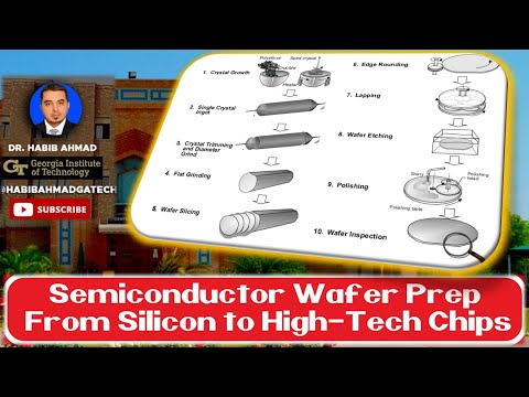
Wafer preparation is a critical step in the semiconductor manufacturing process, as it sets the foundation for the entire production flow. The quality of the wafer surface directly affects the yield and performance of the final device. Semiconductor manufacturing involves a complex series of steps, including wafer fabrication, lithography, and etching. Wafer preparation involves the growth and preparation of the silicon wafer, which is the base material for most semiconductor devices. Silicon wafers are grown using the Czochralski process or the float zone process.
💡 History of Wafer Preparation
The history of wafer preparation dates back to the 1950s, when the first silicon wafers were grown. Over the years, the process has evolved significantly, with advances in cleanroom technology and wafer cleaning techniques. The introduction of chemical mechanical polishing (CMP) in the 1990s revolutionized the wafer preparation process, enabling the production of high-quality wafers with precise surface finishes. CMP has become a crucial step in modern wafer preparation. Semiconductor history is marked by continuous innovation and improvement in wafer preparation techniques.
📈 Evolution of Wafer Sizes
The size of wafers has increased significantly over the years, from 2 inches in the 1960s to 300mm today. This increase in wafer size has enabled the production of more devices per wafer, reducing costs and increasing efficiency. However, larger wafers also pose significant challenges, including wafer warping and thickness variation. Wafer size is a critical factor in determining the yield and performance of semiconductor devices. Yield enhancement techniques are essential to optimize wafer preparation and minimize defects.
🔬 Wafer Cleaning and Etching
Wafer cleaning and etching are critical steps in the wafer preparation process. Wafer cleaning involves the removal of contaminants and impurities from the wafer surface, while etching involves the removal of material from the wafer surface to create patterns and structures. Dry etching and wet etching are two common etching techniques used in wafer preparation. Plasma etching is another technique that offers high precision and control. Surface preparation is essential for successful wafer cleaning and etching.
📊 Wafer Inspection and Metrology
Wafer inspection and metrology are critical steps in ensuring the quality of the wafer surface. Wafer inspection involves the use of various techniques, including optical microscopy and scanning electron microscopy (SEM), to detect defects and contaminants on the wafer surface. Metrology involves the measurement of wafer parameters, such as thickness and surface roughness, to ensure that they meet specifications. CD-SEM is a key technique used in wafer metrology. Defect detection is essential to minimize yield loss and ensure high-quality wafers.
🚀 Wafer Preparation for Advanced Nodes
As the semiconductor industry continues to evolve, wafer preparation must adapt to meet the demands of advanced nodes. Advanced nodes require wafers with precise surface finishes and minimal defects. Extreme ultraviolet lithography (EUVL) is one technique that requires highly precise wafer preparation. FinFET and FD-SOI are other technologies that demand high-quality wafers. 3D ICs and TSV are emerging technologies that will require innovative wafer preparation solutions.
🤝 Collaboration and Standardization
Collaboration and standardization are essential in the semiconductor industry, particularly in wafer preparation. SEMI and IEC are two organizations that play a critical role in developing standards for wafer preparation. Consortia and joint research initiatives are also crucial in driving innovation and standardization in wafer preparation. Industry partnerships are vital to develop new technologies and share best practices. Knowledge sharing is essential to accelerate progress in wafer preparation.
📊 Economic Impact of Wafer Preparation
The economic impact of wafer preparation is significant, as it directly affects the yield and performance of semiconductor devices. Yield loss due to wafer preparation defects can result in significant economic losses. Cost of ownership is a critical factor in wafer preparation, as it affects the overall cost of semiconductor manufacturing. Throughput and cycle time are also important considerations in wafer preparation. Manufacturing excellence is essential to minimize costs and maximize efficiency.
🌎 Environmental Considerations
Environmental considerations are becoming increasingly important in the semiconductor industry, particularly in wafer preparation. Chemical waste and water usage are two significant environmental concerns in wafer preparation. Sustainability is a critical factor in modern wafer preparation, as the industry seeks to minimize its environmental footprint. Green technology and eco-friendly practices are being adopted to reduce waste and minimize environmental impact.
🔮 Future of Wafer Preparation
The future of wafer preparation is exciting, with new technologies and innovations on the horizon. Nanotechnology and artificial intelligence (AI) are two areas that are expected to have a significant impact on wafer preparation. Machine learning and data analytics are being used to optimize wafer preparation and improve yields. IoT and 5G are driving the demand for high-quality wafers and innovative wafer preparation solutions.
📝 Conclusion
In conclusion, wafer preparation is a critical step in the semiconductor manufacturing process, requiring precision, innovation, and collaboration. As the industry continues to evolve, wafer preparation must adapt to meet the demands of advanced nodes and emerging technologies. Wafer preparation is a complex process that involves multiple steps and techniques. Semiconductor manufacturing is a highly competitive industry that demands continuous innovation and improvement.
Key Facts
- Year
- 2022
- Origin
- United States
- Category
- Semiconductor Manufacturing
- Type
- Industrial Process
Frequently Asked Questions
What is wafer preparation?
Wafer preparation is a critical step in the semiconductor manufacturing process that involves the growth and preparation of the silicon wafer. It includes various steps such as wafer cleaning, etching, and inspection to ensure the quality of the wafer surface. Wafer preparation is essential for the production of high-quality semiconductor devices. Semiconductor manufacturing relies heavily on wafer preparation. Yield enhancement techniques are used to optimize wafer preparation and minimize defects.
What are the different types of wafer cleaning techniques?
There are several types of wafer cleaning techniques, including dry cleaning, wet cleaning, and plasma cleaning. Each technique has its own advantages and disadvantages, and the choice of technique depends on the specific application and requirements. Cleaning techniques are critical in wafer preparation to remove contaminants and impurities from the wafer surface. Surface preparation is essential for successful wafer cleaning.
What is the importance of wafer inspection and metrology?
Wafer inspection and metrology are critical steps in ensuring the quality of the wafer surface. Wafer inspection involves the use of various techniques to detect defects and contaminants on the wafer surface, while metrology involves the measurement of wafer parameters to ensure that they meet specifications. CD-SEM is a key technique used in wafer metrology. Defect detection is essential to minimize yield loss and ensure high-quality wafers. Yield enhancement techniques are used to optimize wafer preparation and minimize defects.
What are the challenges in wafer preparation for advanced nodes?
Wafer preparation for advanced nodes requires highly precise surface finishes and minimal defects. Advanced nodes pose significant challenges, including wafer warping and thickness variation. EUVL is one technique that requires highly precise wafer preparation. FinFET and FD-SOI are other technologies that demand high-quality wafers. 3D ICs and TSV are emerging technologies that will require innovative wafer preparation solutions.
What is the economic impact of wafer preparation?
The economic impact of wafer preparation is significant, as it directly affects the yield and performance of semiconductor devices. Yield loss due to wafer preparation defects can result in significant economic losses. Cost of ownership is a critical factor in wafer preparation, as it affects the overall cost of semiconductor manufacturing. Throughput and cycle time are also important considerations in wafer preparation. Manufacturing excellence is essential to minimize costs and maximize efficiency.
What are the environmental considerations in wafer preparation?
Environmental considerations are becoming increasingly important in the semiconductor industry, particularly in wafer preparation. Chemical waste and water usage are two significant environmental concerns in wafer preparation. Sustainability is a critical factor in modern wafer preparation, as the industry seeks to minimize its environmental footprint. Green technology and eco-friendly practices are being adopted to reduce waste and minimize environmental impact.
What is the future of wafer preparation?
The future of wafer preparation is exciting, with new technologies and innovations on the horizon. Nanotechnology and artificial intelligence (AI) are two areas that are expected to have a significant impact on wafer preparation. Machine learning and data analytics are being used to optimize wafer preparation and improve yields. IoT and 5G are driving the demand for high-quality wafers and innovative wafer preparation solutions.